

Mapping Magnetic Fields for EMC Testing of Consumer Electronics
Modern consumer electronics, smartphones, wearables, wireless chargers, laptops, power adapters and smart home devices, pack switching power supplies, wireless charging coils, haptic motors and speaker magnets into a small enclosure. Each of these can radiate a stray magnetic field that couples into nearby traces, cables or other devices and shows up as an EMC problem. A formal radiated emissions test in a compliance chamber tells you whether the product passes or fails, but not which component or trace on the board is actually responsible. Magnetic near-field mapping, taken close to the device under test, fills that gap: it localizes the emitting source so an engineer can fix the root cause before the expensive compliance test, not after a failure.
This article explains what near-field magnetic mapping captures, why it complements formal EMC compliance testing, and how to do it with instruments from SENIS AG, whose special mapper solutions include mappers with inductive probes for 3D mapping of very small AC magnetic fields, down to 100 pT, from below 100 Hz up to hundreds of kilohertz.
What near-field magnetic mapping captures
- Field amplitude and footprint per source. Mapping a grid of points over a PCB or enclosure reveals exactly which inductor, transformer, coil, IC or connector is the dominant emitter, rather than a single pass or fail number for the whole product.
- All three field components (Bx, By, Bz). Distinguishing a loop current source from a leakage field from a coil or a permanent magnet component, such as a speaker or haptic motor, helps point to the right fix: layout change, shielding or component reselection.
- DC and low frequency leakage from magnetic components. Stray field from permanent magnets in speakers, haptic actuators, camera and hinge assemblies, and from wireless charging coils even when idle.
- AC switching frequency emissions. The field generated by a switch mode power supply, DC-DC converter or wireless charging transmitter at its operating frequency and harmonics.
- Design revision comparison. The same map repeated on successive board or enclosure revisions quantifies whether a layout or shielding change actually reduced the emission, before committing to a chamber test.
Why calibrated Hall probes with high frequency bandwidth
Localizing a near-field source at PCB scale needs spatial resolution well below the spacing between traces and components. SENIS Hall probes offer a field-sensitive spot as small as 100 x 100 x 10 µm. The 3-axis versions cover a frequency bandwidth from DC up to 25 kHz, and the 1-axis versions of the same devices reach DC up to 75 kHz. All Hall probes are calibrated in SENIS’ ISO 17025:2017 accredited laboratory, so a map taken today is directly comparable with one taken on a different bench or at a different site.
Approach 1: Bench-top scanning mapper for pre-compliance screening
A general purpose mapper such as the MMS-1A-RS, fitted with the appropriate probe, scans a fixed grid over the PCB, module or enclosure at a constant standoff, building a 2D or 3D magnetic field map of the product. Where the full field image must be captured very quickly, the same task can be performed with the SENIS Magnetic Field Camera, SENCAM, which contains more than 16,000 3-axis Hall pixels, each with a field-sensitive volume of 27 x 9 x 4 µm. This allows the complete magnetic field distribution over an area to be acquired at once, rather than point by point.
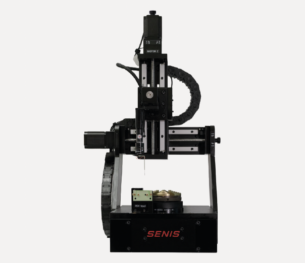
SENIS’ interchangeable probe design lets the same instrument switch between a Hall probe, for DC and low frequency leakage from magnets and coils, and an inductive eddy current probe, for AC emissions at switching frequencies and their harmonics. In practice, the mapper provides the most flexible and traceable pre-compliance investigation, while SENCAM offers a fast full field view for rapid localization of hot spots, design comparison or production screening.
This approach is ideal for a systematic pre-compliance screen: map every candidate source, identify magnetic hot spots, rank them by amplitude and spatial extent, and compare the result against the previous design revision before sending the product to a certified EMC laboratory.
Approach 2: Portable probes for quick bench debugging
During day to day design iteration, engineers often do not need a full calibrated map. They need to quickly confirm which component is radiating before the next board spin. A portable SENIS digital teslameter such as the 3MH1-E, 3MTS, 3MH3, 3MH4 or 3MH6-E, or an analog transducer such as the F3A (detachable probe) or F3B (fixed probe) or the I3D (replacing the I3C), moved by hand over the board while watching the reading, or feeding it to an oscilloscope or spectrum analyzer for frequency content, gives a fast localization at the bench without the setup time of a full scan. The full mapper is then reserved for the formal pre-compliance record on a design that is close to final.
The measurement workflow, step by step
- Define the goal. A quick bench localization during debug, a systematic pre-compliance map ahead of chamber testing, or a comparison between design revisions. This sets whether a portable probe or a full scanning mapper is the right tool.
- Fixture the device under test and define a coordinate grid. Reference the scan grid to the board layout or enclosure outline, so a hotspot in the map can be traced straight back to a specific component or trace.
- Set the standoff and select the probe. Near-field amplitude falls off quickly with distance, so keep a small, consistent standoff, typically a few millimetres above the board, and choose the probe to match the emission type being investigated.
- Choose the range. Match the field range to the strongest expected source, such as a wireless charging coil, so weaker nearby sources are not lost in the noise floor and the strongest source does not clip.
- Define the scan region and step size. Finer steps resolve individual components and traces at the cost of scan time. A coarse first pass followed by a fine pass over the identified hotspot is often the fastest route to a useful answer.
- Acquire the data under realistic operating conditions. Emissions can depend strongly on load, charging state or duty cycle, so scan the device in the operating modes relevant to the failure or the compliance test.
- Visualize and analyze. The SENIS Mapper software builds a field map that can be overlaid on the board layout, making it straightforward to read a hotspot back to a specific component.
- Decide and archive. Rank sources by amplitude, decide on layout or shielding changes, and archive the traceable map to compare against the next revision or against the chamber test result.
Practical tips and common pitfalls
- Keep the standoff constant. Because near-field amplitude decays quickly with distance, comparisons between scans or between design revisions are only meaningful if the probe to board distance is identical each time.
- Separate DC leakage from AC emissions. A speaker magnet’s stray field and a switching converter’s radiated noise are different problems with different fixes. Choosing a probe with the right frequency range keeps the diagnosis clean.
- Match the range to the strongest source so it does not saturate the probe and mask weaker but still problematic emitters nearby.
- Scan under realistic operating conditions, not just at idle. Many of the worst emitters, such as fast charging coils and motors under load, are only active during specific operating states.
- Keep it traceable. ISO 17025 calibrated probes let a design team compare a map from this month’s prototype against one from six months ago, or against a supplier’s board, on the same basis.
- Mapping is diagnostic, not a substitute for compliance testing. Near-field magnetic mapping is a design and pre-compliance tool that helps find and fix root causes efficiently. Formal radiated emissions compliance still requires testing in an accredited EMC chamber against the applicable CISPR, IEC or FCC limits.
Choosing the right instrument, a quick guide
| Need | Recommended SENIS instrument |
|---|---|
| DC and low frequency leakage from magnets, coils and motors | 3-axis Hall probe on a mapper such as the MMS-1A-RS, field-sensitive spot down to 100 x 100 x 10 µm |
| AC switching frequency emissions from converters, transformers, chokes and wireless charging | Analog Hall transducer such as the F3A or F3B (bandwidth from DC up to 25 kHz for the 3-axis versions, DC up to 75 kHz for the 1-axis versions), or a special mapper with inductive probe for very small AC fields up to hundreds of kilohertz |
| Systematic pre-compliance map of a board or enclosure | Bench-top scanning mapper with interchangeable Hall probes |
| Quick bench localization during design debug | Portable digital teslameter or analog transducer |
| Comparing successive design revisions | Same mapper setup and standoff, archived and re-run per revision |
| Production line inspections | SENIS Magnetic Field Camera, SENCAM |
Conclusion
Passing an EMC compliance test starts with knowing where the field is actually coming from. Magnetic near-field mapping, capturing the full Bx, By, Bz vector at a small, consistent standoff over a board or enclosure, turns a pass or fail compliance result into an actionable map of which component or trace needs attention, and lets a design team verify a fix before paying for another chamber test.
A bench-top scanning mapper with interchangeable probes covers systematic pre-compliance screening, while portable teslameters and transducers support fast day to day debugging on the bench. Used together, and with results kept traceable to an ISO 17025 accredited calibration, they let a consumer electronics team find and fix magnetic EMC issues efficiently, as a complement to, not a replacement for, accredited compliance testing.
Next steps
- Explore the full range of SENIS magnetic field mapping systems.
- Discuss your pre-compliance measurement case with our engineers via the contact page.
Instrument specifications may be updated over time. Full and current specifications for each instrument are available on the linked product pages and datasheets. Magnetic near-field mapping is a design and pre-compliance diagnostic tool and does not itself constitute accredited EMC compliance testing.